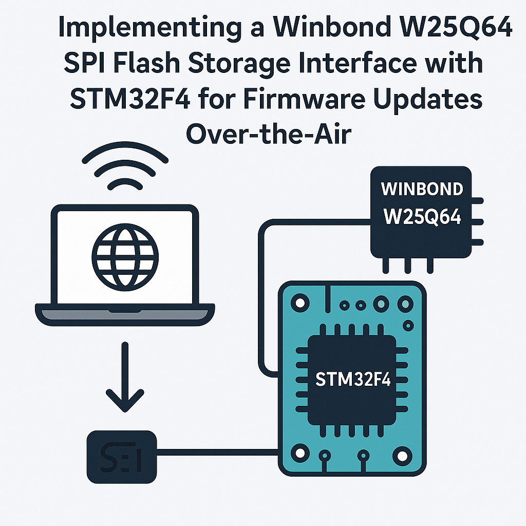
How to Implement Winbond W25Q64 SPI Flash with STM32F4 for OTA Updates
Why External Flash for OTA?
Your STM32F4 has enough flash to run firmware, but not enough to store a second copy while you're updating. That's the problem. You need somewhere to stash incoming firmware during an OTA update, verify it's good, and then swap it in. The Winbond W25Q64 gives you 8MB of SPI flash storage for exactly this purpose — it's cheap, fast, and well-documented.
The basic flow: your device receives new firmware over the network, writes it chunk-by-chunk to the W25Q64, verifies the checksum, and then reboots into the new image. If verification fails, the old firmware stays put. This is the A/B update pattern, and it's how most production devices handle OTA.
What You'll Need
- STM32F4 development board (Nucleo-F446RE, STM32F4 Discovery, etc.)
- Winbond W25Q64 SPI flash chip (or a breakout board with one)
- Jumper wires and a breadboard
- STM32CubeIDE v1.16+ installed and working
- Basic comfort with SPI and the STM32 HAL — you don't need to be an expert, but you should know what a HAL handle is
Wiring: W25Q64 to STM32F4
The W25Q64 uses standard SPI. Here's a typical pin mapping using SPI2 on the STM32F4:
W25Q64 Pin    STM32F4 Pin    Function
----------    -----------    --------
CLK           PB13           SPI2_SCK
DI (MOSI)     PB15           SPI2_MOSI
DO (MISO)     PB14           SPI2_MISO
/CS           PB12           GPIO Output (Chip Select)
VCC           3.3V           Power
GND           GND            Ground
/WP           3.3V           Disable write-protect
/HOLD         3.3V           Disable hold
Watch out: the /WP and /HOLD pins are active-low. Tie them high or you'll get mysterious write failures and bus stalls. I've wasted hours debugging this on a new board — just tie them to 3.3V and move on.
Configuring SPI in STM32CubeIDE
Open STM32CubeIDE, create or open your project, and head to the Pinout & Configuration tab. Enable SPI2 with these settings:
- Mode: Full-Duplex Master
- Data Size: 8 bits
- Clock Polarity (CPOL): Low
- Clock Phase (CPHA): 1st Edge
- NSS: Software (you'll toggle CS manually via GPIO — gives you more control)
- Baud Rate Prescaler: Start with a divide-by-8 or divide-by-16. The W25Q64 handles up to 104MHz, but your board traces and breadboard wiring won't. 10-20MHz is a safe starting point.
Set PB12 as a GPIO Output for your chip select line. Generate the code.
SPI Flash Driver Functions
The W25Q64 has a well-defined command set. You send a command byte, optionally followed by an address and data. Here's the core driver structure:
// Chip select helpers
static void W25Q64_CS_Low(void)  { HAL_GPIO_WritePin(GPIOB, GPIO_PIN_12, GPIO_PIN_RESET); }
static void W25Q64_CS_High(void) { HAL_GPIO_WritePin(GPIOB, GPIO_PIN_12, GPIO_PIN_SET); }

void W25Q64_Init(void) {
    W25Q64_CS_High();  // Deselect by default
    HAL_Delay(10);     // Let the chip wake up after power-on

    // Read the JEDEC ID to verify communication
    uint8_t cmd = 0x9F;
    uint8_t id[3];
    W25Q64_CS_Low();
    HAL_SPI_Transmit(&hspi2, &cmd, 1, HAL_MAX_DELAY);
    HAL_SPI_Receive(&hspi2, id, 3, HAL_MAX_DELAY);
    W25Q64_CS_High();
    // id should be {0xEF, 0x40, 0x17} for W25Q64
}

void W25Q64_WriteEnable(void) {
    uint8_t cmd = 0x06;
    W25Q64_CS_Low();
    HAL_SPI_Transmit(&hspi2, &cmd, 1, HAL_MAX_DELAY);
    W25Q64_CS_High();
}

void W25Q64_WaitBusy(void) {
    uint8_t cmd = 0x05, status;
    W25Q64_CS_Low();
    HAL_SPI_Transmit(&hspi2, &cmd, 1, HAL_MAX_DELAY);
    do {
        HAL_SPI_Receive(&hspi2, &status, 1, HAL_MAX_DELAY);
    } while (status & 0x01);
    W25Q64_CS_High();
}

void W25Q64_EraseSector(uint32_t addr) {
    W25Q64_WriteEnable();
    uint8_t cmd[4] = { 0x20, (addr >> 16) & 0xFF, (addr >> 8) & 0xFF, addr & 0xFF };
    W25Q64_CS_Low();
    HAL_SPI_Transmit(&hspi2, cmd, 4, HAL_MAX_DELAY);
    W25Q64_CS_High();
    W25Q64_WaitBusy();  // Sector erase takes ~60ms
}

void W25Q64_PageProgram(uint32_t addr, uint8_t *data, uint16_t size) {
    W25Q64_WriteEnable();
    uint8_t cmd[4] = { 0x02, (addr >> 16) & 0xFF, (addr >> 8) & 0xFF, addr & 0xFF };
    W25Q64_CS_Low();
    HAL_SPI_Transmit(&hspi2, cmd, 4, HAL_MAX_DELAY);
    HAL_SPI_Transmit(&hspi2, data, size, HAL_MAX_DELAY);
    W25Q64_CS_High();
    W25Q64_WaitBusy();
}

void W25Q64_Read(uint32_t addr, uint8_t *buffer, uint16_t size) {
    uint8_t cmd[4] = { 0x03, (addr >> 16) & 0xFF, (addr >> 8) & 0xFF, addr & 0xFF };
    W25Q64_CS_Low();
    HAL_SPI_Transmit(&hspi2, cmd, 4, HAL_MAX_DELAY);
    HAL_SPI_Receive(&hspi2, buffer, size, HAL_MAX_DELAY);
    W25Q64_CS_High();
}
A few things to note: you must call WriteEnable before every write or erase operation — the chip auto-clears the write-enable latch after each one. And page programming is limited to 256 bytes at a time. If you need to write more, split it across page boundaries. Going past a page boundary wraps around to the start of that page and overwrites your data.
Building the OTA Update Logic
With the flash driver working, here's how the OTA flow comes together:
- Receive firmware: Your device gets the new binary over whatever transport you're using — HTTP, MQTT, BLE, UART, doesn't matter. What matters is you can receive it in chunks.
- Erase the target region: Before writing, erase the sectors where the firmware image will live. The W25Q64 has 4KB sectors. Calculate how many you need based on the firmware size and erase them upfront.
- Write chunks to flash: As firmware data arrives, write it to the W25Q64 using page programming. Keep a running CRC32 as you go.
- Verify integrity: Once the full image is written, read it back and compare the CRC32 against the expected value sent by the server. Don't skip this step — flash writes can fail silently.
- Signal the bootloader: Write a flag to a known location (either in the W25Q64 or the STM32's internal flash) telling the bootloader a valid update is waiting. Then trigger a system reset.
- Bootloader copies and boots: Your bootloader reads from the W25Q64, writes to the STM32's internal flash, and jumps to the new firmware. Consider using MCUboot if you want a production-grade bootloader with rollback support.
Tip: always store a firmware header at the beginning of the image in external flash. Include the firmware version, size, CRC32, and a magic number. Your bootloader should validate all of these before copying anything.
Troubleshooting
- Can't read the JEDEC ID (returns 0xFF or 0x00): Double-check your wiring, especially MISO/MOSI order. Also verify your SPI clock speed isn't too fast for your physical setup — long breadboard wires add capacitance. Drop to a slower prescaler and try again.
- Writes seem to work but reads return garbage: You probably forgot to erase before writing. Flash memory can only flip bits from 1 to 0 during a write. You need a sector erase (which sets everything to 0xFF) before programming.
- OTA image boots once then bricks: Your bootloader is probably overwriting the update flag before verifying the new firmware actually runs. Implement a "mark as good" step in your application firmware, and have the bootloader roll back if it doesn't see that flag after a reset.
- SPI communication works intermittently: Check that /WP and /HOLD are tied high. Also make sure your CS line isn't floating during startup — configure it as a push-pull GPIO output and set it high before initializing SPI.
Where to Go From Here
This gets you a working SPI flash driver and the bones of an OTA system. For production, you'll want to add encryption (AES-256 on the firmware image), signature verification (ECDSA), and a proper dual-bank bootloader. MCUboot handles most of this out of the box if you don't want to roll your own. Also consider adding wear-leveling if you'll be writing to the same flash regions frequently — the W25Q64 is rated for 100K erase cycles per sector, which sounds like a lot until your device starts updating daily.